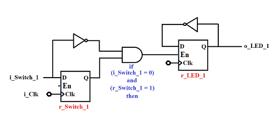
Somehow the circuit needs to maintain the current state of LED 1. It must also be able to detect the moment when button 1 goes from 1 (high, depressed) to 0 (low, released). In order to implement those kinds of features, another (fundamental) component of the FPGA's logic element is required: the d-flip-flop, or "register".
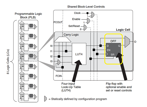
A clock signal is one of the inputs, and whenever a rising edge or falling edge occurs in the clock signal, the D input is "latched" to the Q output. These can be configured to latch on only the rising edge of the clock. All d-flip-flops in the system get updated simultaneously.
There is also a SET/RESET input that will set Q (either synchronously with the clock or immediately, i.e. asynchronously). The value the register is reset to can be configured to be either 1 or 0 at design time.
Most importantly (for this project) there is a Clock Enable (EN) input to the register which can effectively "disconnect" the clock pulse for a period of time, allowing the register to retain it's memory indefinitely, without worry to the fluctuating input on D.
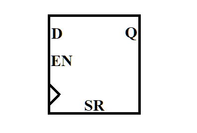
Here's a diagram of how input D is latched to output Q only the rising edge of the clock signal: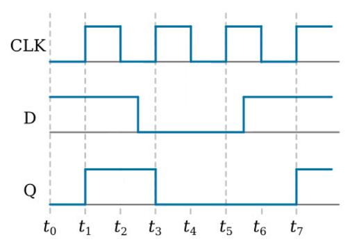
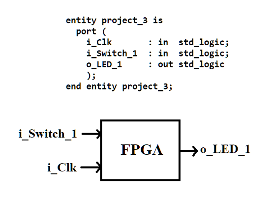
The "entity" section of the VHDL source file will contain the external connections the FPGA will be using that connect to the various parts of the Go Board. Here we're using the signal from button 1, the clock that is onboard (25 MHz), and the signal that goes to LED 1.
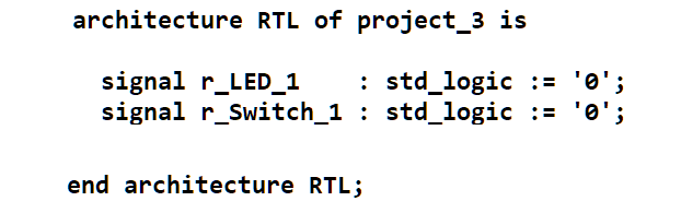
The way a d-flip-flop is implemented in code, you first have to declare "signals" in the architecture section, one for each d-flip-flop that will be needed. For this project, we need one register to track the state of i_Switch_1 (so that the previous time-slice's state can be compared to the current time-slice's state, i.e. edge detection). We need a second register to maintain the state of LED_1 between button releases.
Interestingly, this alone doesn't create the d-flip-flop. For that, we need to add a "process" block:
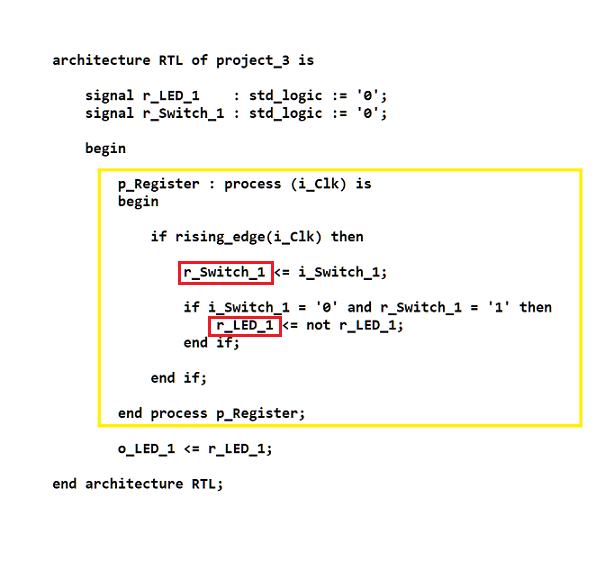
The process block above (yellow box) defines a single clock in the sensitivity list. This means that the statements within the process block will ONLY execute when there is a change in state in that signal in the sensitivy list (and this particular one uses a library function to detect on the rising edge of each clock cycle).
The red boxes are were the actual d-flip-flops are "created" by the iCEcube2 compiler. Since they are being assigned within a clocked process block, they will be implemented as registers.