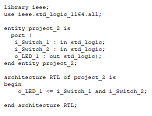
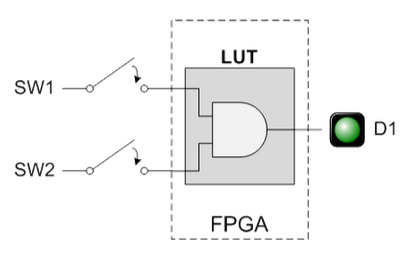
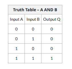
Project 2: Implement an AND Gate with a Look Up Table (LUT)
-
Page maintained by Darron Vanaria
Return to Main FPGA Project Page
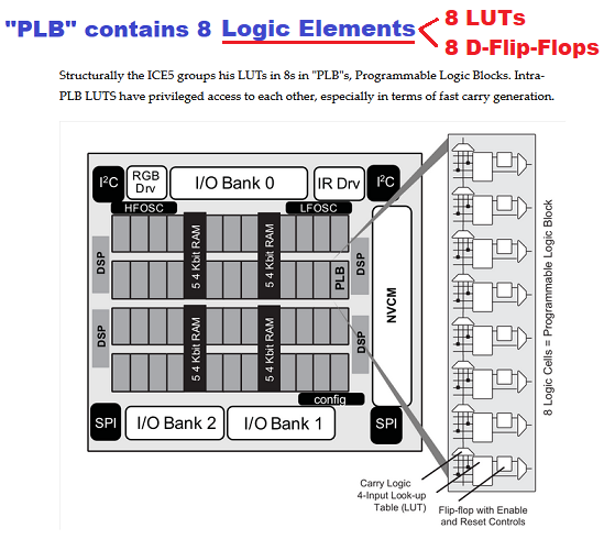
The two "workhorses" of FPGAs are the LUT (Look Up Table) and the D-Flip-Flop (or register). There are no individual logic elements in an FPGA (like AND gates and OR gates) - instead, logic circuits are implemented as a series (a table) of inputs and desired outputs.
The iCE40 HX1K has 1024 "logic elements" - and each logic element contains both a 4-input LUT and a Register. On a higher level, there are 8 logic elements arranged into a block called a PLB (Programmable Logic Block):