The Constraints File
After the synthesis step, iCEcube2 will need a constraints file in order to resolve top-level FPGA pins to the design. For the Nandland Go board, the constraints file can be found on the Nandland website, or copy it directly from here:
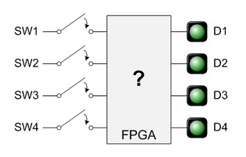
The constraints file contains the physical pin assignments for the following signals:
- 1 pin for FPGA Clock
- 4 pins for LEDs
- 4 pins for Switches (push buttons)
- 14 pins connect to two 7-segment displays
- 2 pins connect to UART
- 11 pins for VGA Output (HSync, VSync, 3 each for R,G,B)
- 8 pins for PMOD Signals
VHDL Solution
This is a pretty straightforward solution, tying each push-button signal directly to it's corresponding LED: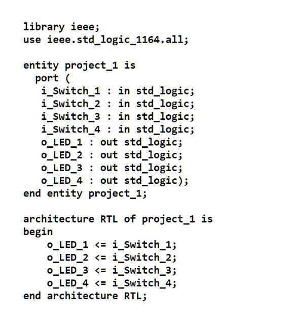
Solution Files:
Workflow in iCEcube2
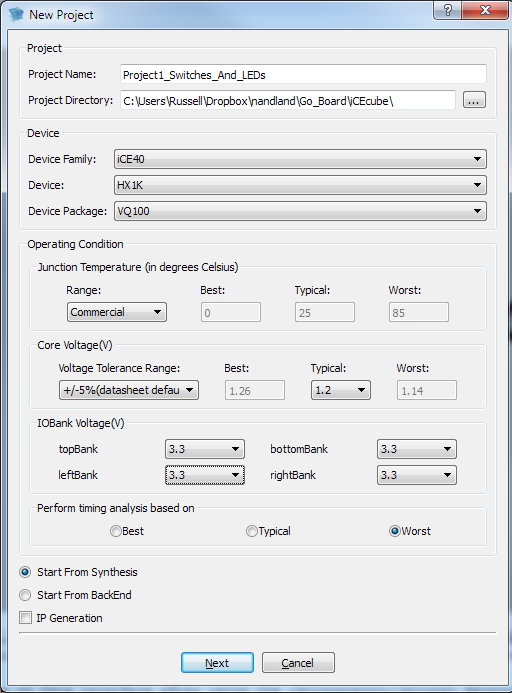
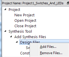
- Start a New Project
- Add source code files
- Run Synthesis
- Run Place and Route
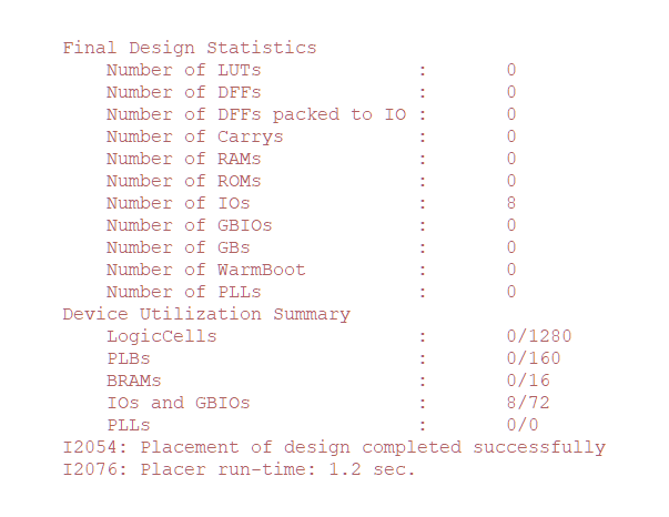
- Check resources used (when P&R completes)
- Generate bitstream
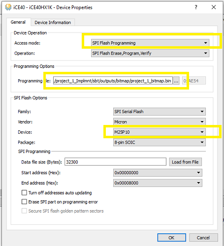
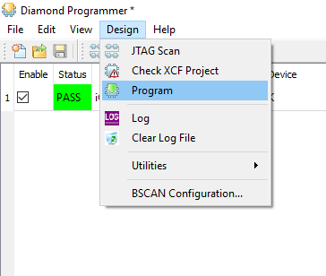
- Use the Diamond Programmer to load the bitstream file onto the FPGA board.
- Test on the actual hardware!
- Synthesis converts the VHDL or Verilog code into physical elements that
are available on your particular FPGA. An FPGA has dedicated pieces of
logic on it. It has wires, Look-Up Tables, Registers, and Memory. It can have
other things, but these are by far the
most targeted elements during synthesis.
- Place and Route takes those components and places them on your FPGA. You can think of an FPGA as a large grid of these components. Place and Route will assign which component gets used where. It is a particularly important step of the FPGA build process for designs that use clocks.
This is the step where the Constraints file becomes important.
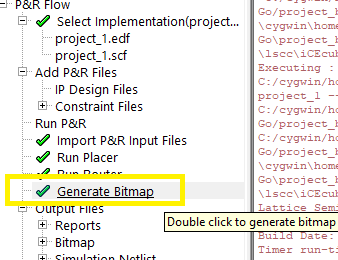
The .bin file is located here: project\project_Implmnt\sbt\outputs\bitmap
Return to Main FPGA Project Page